
Online AC/DC test and AOI for SiC wafer-level die
WAFER · DIE SELECTION
Known Good Die Test System
Automated AC/DC and visual screening for SiC wafer-level die, separating good and defective devices before module integration.
MODEL / PLATFORMKGD / CP PLATFORM
Start an enquiry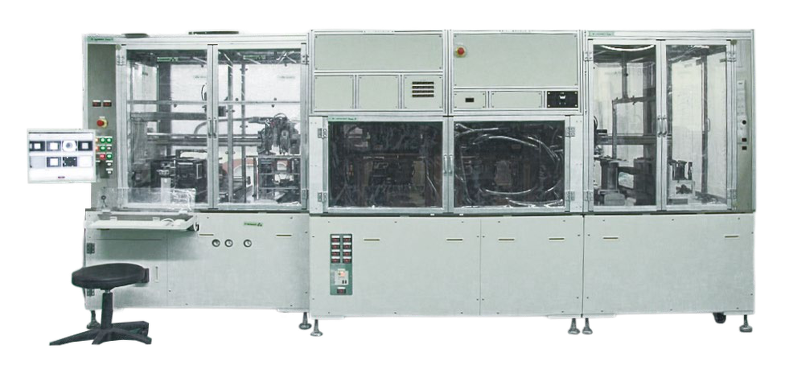 Company catalogue reference · P16–17
01KGD / CP PLATFORMPLATFORM
02SiC wafer CPTypical applications
03Up to 1200 UPHThroughput
04P16–17Company catalogue reference
System highlights
Wafer cassette, tray and contact method are configured around the customer process.
Automated wafer-cassette supply, die pickup and tray loading
Good/defective die classification with controlled heating
Support for UV / blue-film wafers and multiple wafer sizes
Catalogue specifications
Known Good Die Test System
Technical data shown is based on the current WYJ product catalogue. Final configuration is application-specific.
01Throughput
Up to 1200 UPH
02Wafer formats
6 / 8 / 12 inch cassette options
03Die size
4 × 4 to 25 × 25 mm
04Die thickness
70–500 μm
05Dynamic bus
Up to 3000 V, upgradeable
06Device coverage
MOSFET · IGBT · FRD · Si · SiC
Typical applications
Device coverage
01SiC wafer CP
02Known-good-die selection
03Module yield improvement
04Automated die handling
APPLICATION ENGINEERING · SHENZHEN